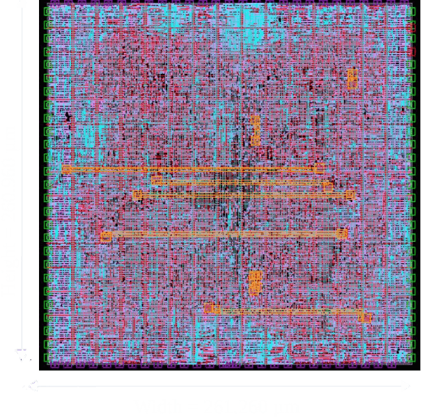
APB (Advanced Peripheral Bus) IP is a reusable intellectual property (IP) block that implements the APB protocol for efficient communication with low-power peripherals. It simplifies the integration of devices like UARTs, timers, and GPIOs in SoCs by providing a simple, low-latency interface. APB IP ensures compliance with AMBA standards and supports easy interfacing with higher-performance buses like AHB or AXI through bridges.


| Name | Direction | Width | Description |
|---|---|---|---|
| PCLK | Input | 1 | Global clock |
| PRESETN | Input | 1 | Global reset |
| PSEL_M/PSEL_S* | O & I | 2 | Select signal in Master and Slave |
| PENABLE_M/PENABLE_S* | O & I | 2 | Enable signal distinguishes between setup and access phase |
| PSTRB_M/PSTRB_S* | O & I | 8 | Which byte lane of write data is valid during write operation in Master and Slave |
| PWAKEUP_M/PWAKEUP_S* | O & I | 2 | Indicates any activity associated |
| PADDR_M/PADDR_S* | O & I | 64 | Address for write and read in Master and Slave |
| PWDATA_M/PWDATA_S* | O & I | 64 | Write data in Master and Slave |
| PRDATA_M/PRDATA_S* | I & O | 64 | Read data in Master and Slave |
| PSLVERR_M/PSLVERR_S* | I & O | 2 | Indicates slave error when address is out of range in Master and Slave |
| PREADY_M/PREADY_S* | I & O | 2 | Indicates that write and read transaction will perform after it goes high in Master and Slave |
| PWRITE_M/PWRITE_S* | O & I | 2 | Indicates whether write or read has to be performed in Master and Slave |
| m_generic bus interface | O / I | 8 | Interface signals to and from the master |
| s_generic bus interface | O / I | 8 | Interface signals to and from the Slave |
| Name | Direction | Width | Description |
|---|---|---|---|
| PCLK | Input | 1 | Global clock |
| PRESE
TN |
Input | 1 | Global reset |
| PSEL_M /PSEL_S* |
O & I | 2 | Select signal in Master and Slave |
| PENABLE_M /PENABLE_S* |
O & I | 2 | Enable signal distinguishes between setup and access phase |
| PSTRB_M /PSTRB_S* |
O & I | 8 | Which byte lane of write data is valid during write operation in Master and Slave |
| PWAKEUP_M /PWAKEUP_S* |
O & I | 2 | Indicates any activity associated |
| PADDR_M/ PADDR_S* |
O & I | 64 | Address for write and read in Master and Slave |
| PWDATA_M/ PWDATA_S* |
O & I | 64 | Write data in Master and Slave |
| PRDATA_M/ PRDATA_S* |
I & O | 64 | Read data in Master and Slave |
| PSLVERR_M /PSLVERR_S* |
I & O | 2 | Indicates slave error when address is out of range in Master and Slave |
| PREADY_M/ PREADY_S* |
I & O | 2 | Indicates that write and read transaction will perform after it goes high in Master and Slave |
| PWRITE_M/ PWRITE_S* |
O & I | 2 | Indicates whether write or read has to be performed in Master and Slave |
| m_generic bus interface |
O / I | 8 | Interface signals to and from the master |
| s_generic bus interface |
O / I | 8 | Interface signals to and from the Slave |
Ready to discuss your IP Solutions needs? Contact us to schedule an appointment with one of our experts.